In this lab activity you will examine the properties of pn-junction diodes and use diodes to convert AC signals to DC signals.
Introduction to PN-Junction Diodes
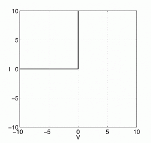
A diode is a device that only allows current to flow in one direction. For this reason, an ideal diode has a current voltage plot that looks like this.
Note that by Ohm’s law, the inverse of this plots slope is the diodes resistance. So a diode has infinite resistance if the voltage applied to it is negative but has zero resistance if the voltage applied to it is positive.
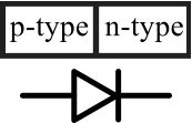
It is possible to construct a nearly-ideal diode by binding a piece of N-type semiconductor to a piece of P-type semiconductor together. Because of the nature of the P-type and N-type semiconductors, the junction between the two semiconductors creates a zone depleted of charge carriers. We will cover the physical details of what is going on here in class but the practical result of this depletion zone is that charge can only move in one direction through the PN-junction. Below is a schamatic symbol for a PN-junction diode.
In order for current to flow through the diode, the voltage supplied to the P-type side of the diode (the anode) must be higher then the voltage supplied to the N-type side (the cathode). Current flows through the diode in the direction of the arrow. The cathode of a diode is always labeled with a strip or negative sign.
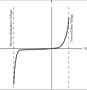
The following is a representative current voltage plot for a real PN-junction diode.
Note that if the voltage is sufficiently negative current will flow through the diode in the reverse direction. This voltage is referred to as the breakdown voltage and is actual sometimes useful. A Zener diode has a reliably known reverse breakdown voltage and can be used to limit the maximum voltage in circuits. On the other hand, notice that a small positive voltage is needed to get current to flow in the forward direction. This forward bias voltage is needed to overcome the PN-junction depletion region and is about 0.5-0.7 V for diodes made from silicon and about 0.3 for diodes made of germanium.
Diode Circuits
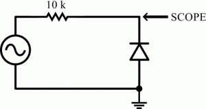
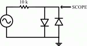
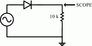
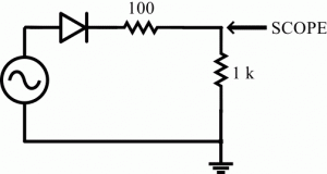
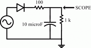
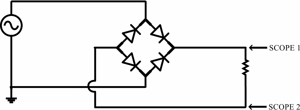
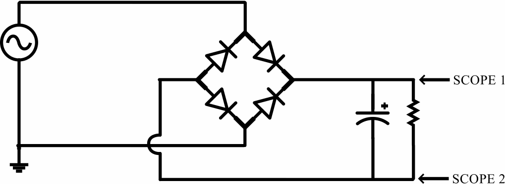
Construct each of the following circuits using small signal silicon diodes (1N4148). For each circuit use the sine wave generator on your digital/analog trainer set to a frequency of 1 kHz as the signal source. Attach your oscilloscope to the location(s) labeled “SCOPE” and draw the signal you see on the scope in your lab notebook. Above each drawing, also show the schematic of the circuit being tested. Sometimes you will draw two signals superposed on top of each other using channels 1 and 2. Make sure the vertical scales are the same before drawing these two-trace outputs. Explain why the signal looks the way it does below each drawing.
