Background
The field of electronics is essentially one of applied physics. Modern civilization is possible because scientists and engineers are able to utilize the laws of electromagnetism to build electrical devices capable of doing useful things. Some of the most significant electrical devices of the modern era are digital devices and digital computers. This laboratory is designed to introduce you to digital electronics. Since our way of life depends on such devices, it is important to have some knowledge of how these devices work. The digital devices you will experiment with are integrated circuits (ICs) or “chips” of the 7400 series of TTL (transistor-transistor logic) circuits originally designed in the 1960s and used to build mainframe computers in the 1960s and 1970s. These digital ICs are designed to perform one of the basic logic operations (AND, OR, NAND, NOR, etc.). The 7400-series ICs you will use today each have a total of 4 logic gates on them. The CPUs and memory chips in modern computer may have well over one hundred million logic gates. However, these modern ICs use circuits that perform the same logic operations as the nearly 50 year old 7400 series.
Truth Tables
A) Complete the following truth tables for the AND, OR, NAND, NOR, XOR operations. A and B are the inputs and OUT is the output. In digital electronics, low voltage (L) corresponds to the binary number 0 and the Boolean value of false. High voltage (H) corresponds to the number 1 and the value of true. Draw the schematic symbol for the corresponding logic gate next to its respective truth table.
| AND | ||
| A | B | OUT |
| OR | ||
| A | B | OUT |
| NAND | ||
| A | B | OUT |
| NOR | ||
| A | B | OUT |
| XOR | ||
| A | B | OUT |
Truth Tables of 7400 Series ICs
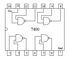
The 7400 has four identical logic gates that perform one of the logic operations above. The pin read out for the 7400 is shown below. The inputs and the outputs of the four individual logic gates are labeled in addition to the +5 V and 0 V pins that need to be connected to your power supply in order for the chip to work.
B) Build a circuit to determine the truth table for the 7400. Use an LED connected to a 20 to 40 Ω resistor to monitor the output (follow the schematic drawn by the instructor). Remember that high voltage (+5 V) is true and low voltage (0 V) is false. Construct the truth table for the 7400. What logic operation does the 7400 perform? Draw the schematic symbol for this logic gate next to its truth table and label it?
C) Repeat part (B) using the 7402 and the 7432 ICs (search google for datasheets for pin out diagrams).
D) Construct the circuit below using two of the individual NOR gates using one of the chips studied above. Notice that the output of one of the gates is the input to the second gate. Using your previous results, construct the truth table for this circuit. Then, build the circuit and test to make sure that your truth table is correct.
| Truth Table | |||||
| A | B | C | X | OUT predicted | OUT experimental |
A Data Latch Circuit
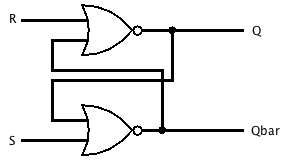
E) Construct the circuit below using two individual NOR gates. Notice that the output from each gate is an input to the other gate. This feedback allows this “data latch” circuit to act as a simple memory circuit. Connect R and S to data switches on an analog/digital trainer board, build the circuit, and test it to complete the following truth table.
| Data Latch Circuit | |||
| R | S | Q | Qbar |
| L | H | ||
| H | L | ||
| H | H | ||
F) With S low and R high, move R to low. What happens to Q and Q bar?
G) Move S high then back to low. What happens to Q and Q bar?
H) Move R high then back to low. What happens to Q and Q bar?
I) Why isn’t R and S both low included on the truth table?
J) In light of the previous three questions, describe how this data latch circuit can function to store one bit of information, that is, one value that is either a zero or a one.


