The ATmega328 used on the Arduino Uno has 14 digital input/output pins (two are used for serial communication). What if you need more than 14 digital inputs/outputs? One solution is to use an 8-bit shift register like the 74HC595 integrated circuit. This chip has 8 output pins that can be set to high or low depending on the value of an 8-bit number stored in the chip’s 8-bit storage register. Importantly, this 8-bit number can be sent in serial to the chip in the form of a binary number via an 8-bit shift register and the chip converts this serial input to a parallel output. For example, if the number 197 is sent to the chip (binary 11000101) then output pins 0, 2, 6, and 7 will be set high while output pins 1, 3, 4, and 5 remain low. The chip also has a data latch pin which when set high prevents the outputs from changing. The order of events to get pins 0, 2, 6, and 7 to go high is as follows. First the data latch pin (pin 12) is set to low. If the data latch pin remains high, any changes to the shift register will immediately be reflected on the output pins. By setting the latch pin low we can change the register and hide the changes until we are finished, making it appear like we have individual control over all of the outputs. Then each digit in the number (11000101) is sent to the serial input pin (pin 14) one at a time starting with the most significant bit. Pin 14 set high corresponds to a one and pin 14 set low corresponds to a zero. To store each bit in the serial input clock pin (pin 11) is toggled high then low. Finally the data latch pin is set high to display the contents of the shift register on the eight parallel output pins.
Another way of thinking about this process is that every time the serial clock pin is set high, the bits in the shift register shift one place to the left and the most significant bit drops off. The least significant bit is set to whatever the serial input pin is set to. So if the number is the shift register is 01110001, the serial input pin is set high (1), and the serial clock is toggled high, the number stored in the shift register becomes 11100011. When the data latch pin is set high, whatever is currently stored in the shift register is transferred to the output register and the output pins reflect this value. For this reason, we can execute several shifts before displaying the changes on the output pins creating the illusion that we have individual control over every individual output pin.
In conclusion, the ‘595 shift register allows one to take a serial input (a series of zeros and ones) and produce a parallel output.
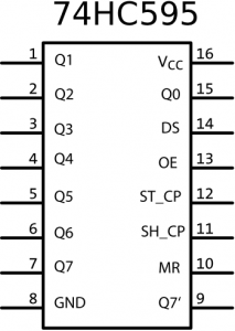
Below is the pinout diagram for the 74HC595 IC. Notice that pins MR and OE must be connected to 5 V and 0 V, respectively, for normal operation.
74HC595 Pinout Diagram
A full data sheet for the 74HC595 can be found here.

Q0-Q7 – Output Pins
Vcc – 5 V
GND – 0 V
ST_CP – storage register clock pin
SH_CP – shift register clock pin
OE – disables outputs if set high (must be connected to 0 V for normal operation)
DS – serial data input pin
MR – clears shift register if set low (must be connected to 5 V for normal operation)
Q7′ – allows more than one chip to be daisy-chained together by sending the most significant bit to another 75HC595’s DS pin allowing for the effective creation of 16-bit (2 chips), 24-bit (3 chips), or larger storage registers.
Use the 74HC595 to Light Up LEDs
Place a ‘595 shift register on an analog/digital trainer board. Connect the chip to power and ground. Connect LEDs on output pins Q0 to Q7 (don’t forget to use current limiting resistors). Connect MR to 5V (high) and OE to ground (low). Connect the ST_CP, SH_CP, and DS pins to three switches on the trainer board. With knowledge of the rules governing the ‘595’s operation given above, toggle the three switches in a sequence necessary to get the LEDs to display the binary number 10110100..
Use the 74HC595 to Control a Seven-Segment LED Display
The PDF below is the datasheet for a 7-segment LED display. This display is uses a common cathode (one path to ground) configuration.
Don’t forget to use current limiting resistors and hook up the seven segments (a through g) of the display to outputs Q0 through Q6 on the ‘595 on the analog/digital trainer board. Notice that pin 2 and 9 on the display need to be connected to ground (it is a common cathode design). Use the rules governing the ‘595’s operation to get the display to show the digit 3.
Assignment
Use two ‘595 shift registers, two 7-segment displays, and the myShiftOut() function (follow this link to learn more about this function) to make a circuit and program that counts from zero to 19 then repeats. Use the delay() function to configure the circuit to take about 20 seconds to count from 0 to 19.
To accomplish this the two shift registers must be daisy chained together.